
Seminar on CMOS IC fabrication for young researchers was held at Hiroshima University
As an activity of RCBE (Research Center for Biomedical Engineering), the seminar of CMOS IC has been arranged for young researchers. The seminar was held at Hiroshima University from August 19th to 24th this year.
Participants this year were 13 people: 8 members from the practical training program for semiconductors, 2 students from university and technical college for the nanotech platform program, 2 internships form college students, and 1 student of Hiroshima University.
Fabricated devices in this training course are CMOS inverters, NAND and NOR circuits based on n-MOS and p-MOS transistors of Al gate. Attendances can design any kinds of circuit (there was a student who designed a half adder this year). The minimum design rule is 3 μm because of the DMD (digital micro-mirror device) maskless exposure system.
On the first day, the attendances designed their own circuits using layout-design-tool. They manufactured the designed devices in the super-clean-room in next three days, and measured the electric characteristics in last two days. The measurement time had been strictly restricted last year because of 24 members. However, we could evaluate each device well this year by limiting the attendances. This training will be continued and is opening to every researcher.
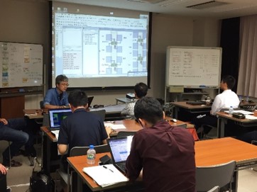 Designing circuits |
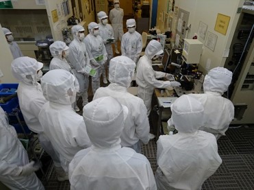 In the super-clean-room |
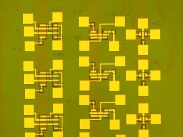 Fabricated CMOS device |
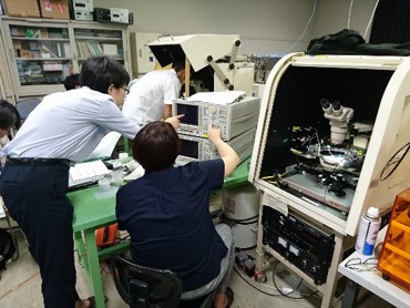 Measuring electric characteristics |